LM40PB-L
40 nm planar bulk, low power
First development release (0.1.0-dev).
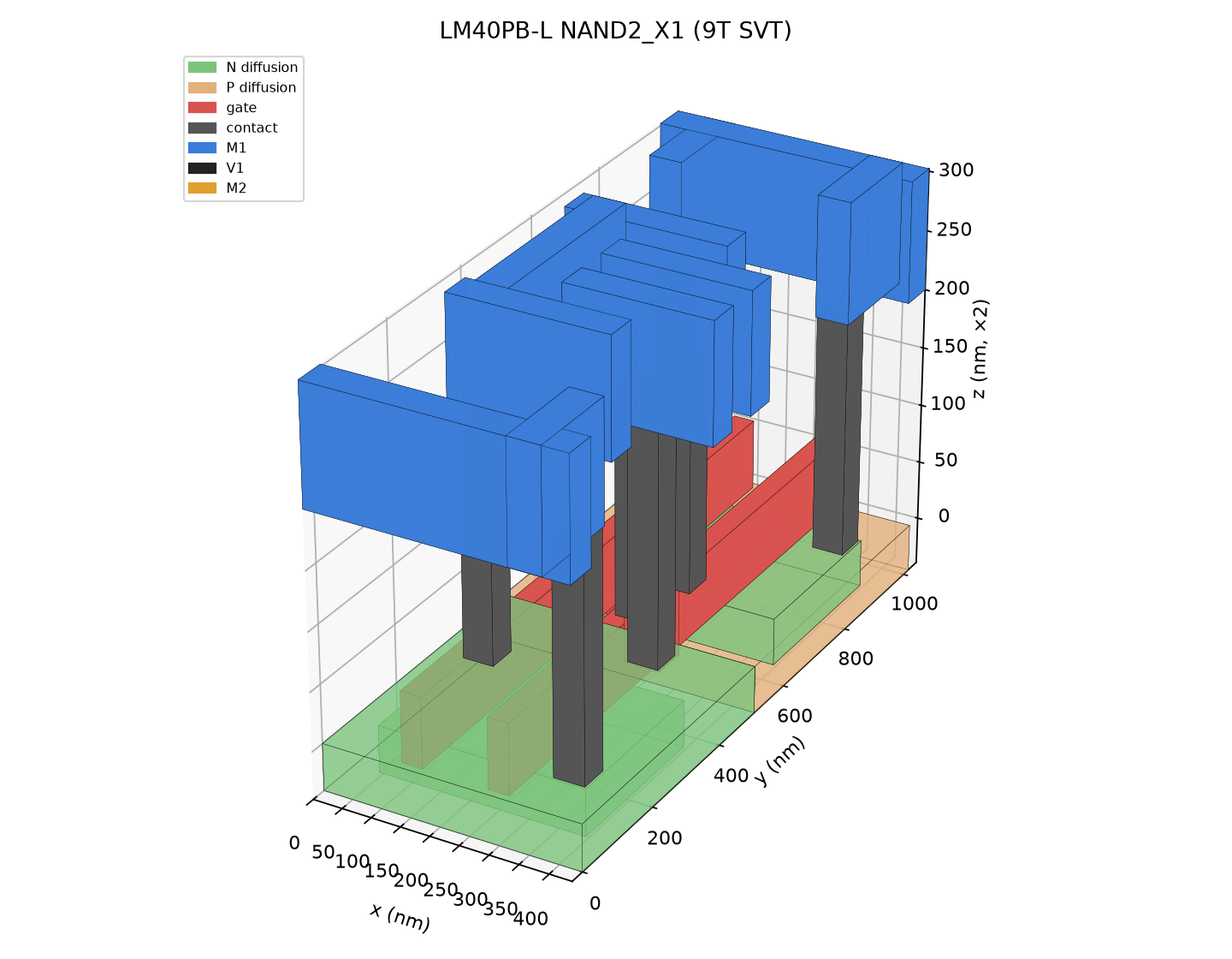
LM40PB-L is a complete 40 nm-class low-power kit: planar bulk transistors with a silicon-oxynitride gate oxide, three threshold-voltage flavours, two cell heights and a nine-layer copper interconnect. It is the reference kit of the family and the first one taken all the way to characterized and checked libraries.
Why 40 nm
The 40 nm generation remains one of the most used technologies in production: microcontrollers, connectivity, power management, automotive and IoT chips. It is also the last generation of the classic planar transistor, which makes it the natural baseline for every comparison in our family: what changes when the gate wraps around the channel, when wires get narrower, when the supply drops.
Technology at a glance
| Supply | 1.05 V nominal; 0.95 and 1.15 V corners |
| Contacted gate pitch | 146 nm |
| Gate length | 32 nm (LVT), 35 nm (SVT), 38 nm (HVT) |
| Gate oxide | SiON, 1.2 nm physical, 1.83 nm electrical |
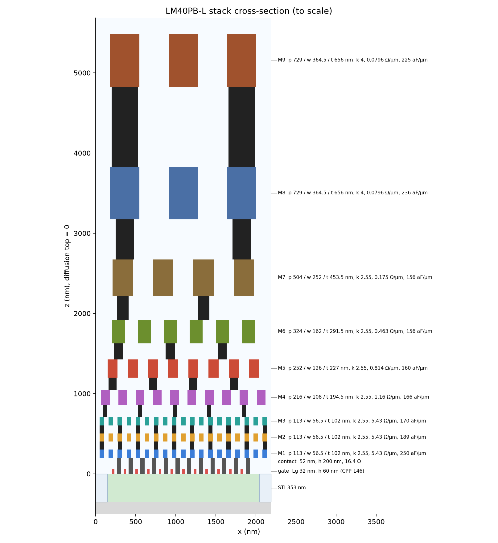
| Metal stack | 9 copper layers, 113 nm minimum pitch, low-k dielectric |
| Cell heights | 9 tracks (1017 nm) and 12 tracks (1356 nm) |
| Threshold voltages | HVT, SVT, LVT |
| Device model | BSIM4 |
Transistors
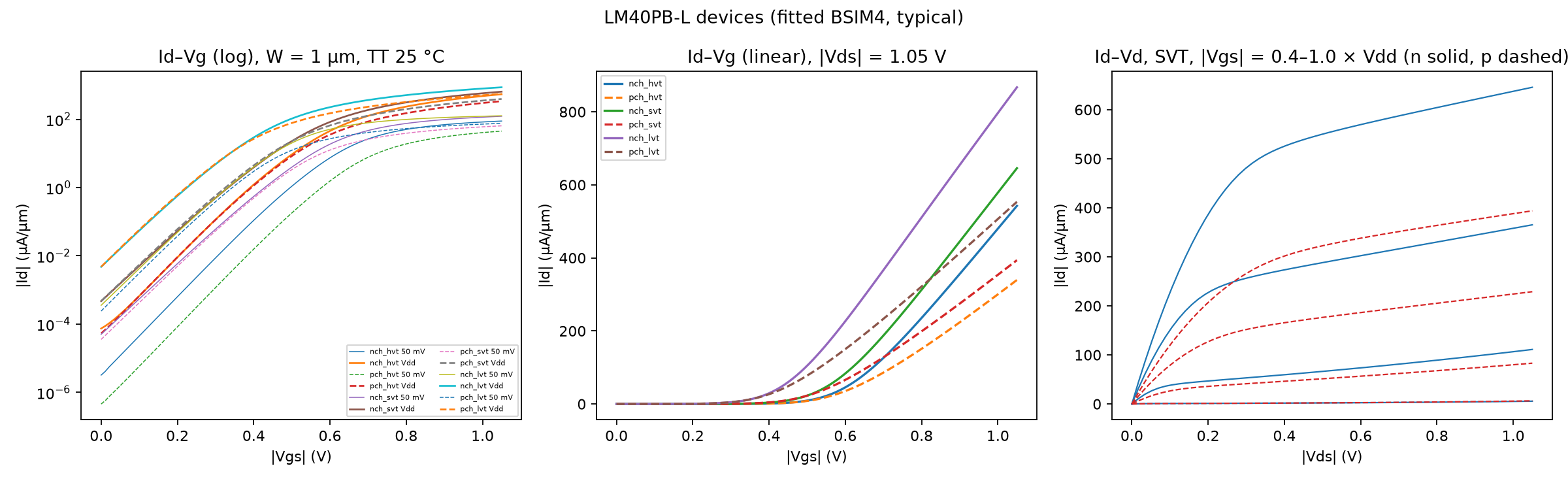
Each flavour is fitted to cited targets for off-state leakage and on-state drive, and to cited gate capacitance, so that both speed and switching energy are realistic.
| Device | Leakage (nA/µm) | Drive (µA/µm) |
|---|---|---|
| nMOS HVT / SVT / LVT | 0.05 / 0.5 / 5 | 536 / 638 / 700 |
| pMOS HVT / SVT / LVT | 0.05 / 0.5 / 5 | 335 / 389 / 438 |
Interconnect
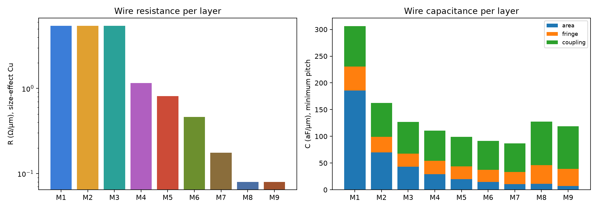
Nine copper layers, from 113 nm pitch for local wiring to 729 nm for power. Resistance includes the size effect of narrow copper lines (surface and grain-boundary scattering), and vias are modelled with an interface term calibrated on a published 45 nm reference.
Standard cells
- 130 cells per library: inverters and buffers, NAND/NOR/AND/OR with 2–4 inputs, AOI/OAI from 21 to 222, MUX, XOR/XNOR, latch, flip-flops with and without reset, clock gate, tie, fill, well tap and decoupling cells; drive strengths X1–X8.
- 9-track libraries in all three threshold flavours: a NAND2 gate density of about 2.2 million gates per mm².
- 12-track library with about 40 % stronger transistors per cell for performance-critical blocks (timing characterization in progress).
Timing and power
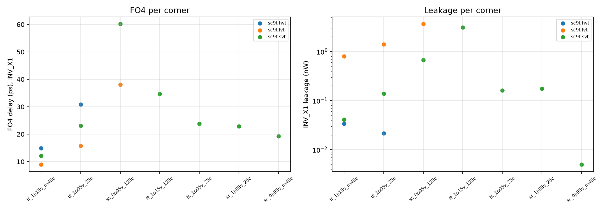
The 9-track libraries are characterized at 13 process, voltage and temperature corners: all five process corners for SVT, and typical, slow hot and fast cold for HVT and LVT. A fanout-of-four inverter delay at the typical corner is about 23 ps (SVT) and 16 ps (LVT).
Verified
- Every cell from its drawn layout: extracted independently and tested for its logic function, 130/130 per library.
- Against 45 nm-class references it was not fitted to (gate capacitance, delay per stage, drive, input capacitance, via resistance, cell area): all within band.
- Against transistor-level simulation of real logic paths (an 8×8 multiplier and a counter, driven by real input vectors): the timing libraries are on the safe side throughout, with a mean deviation of about 2 %.
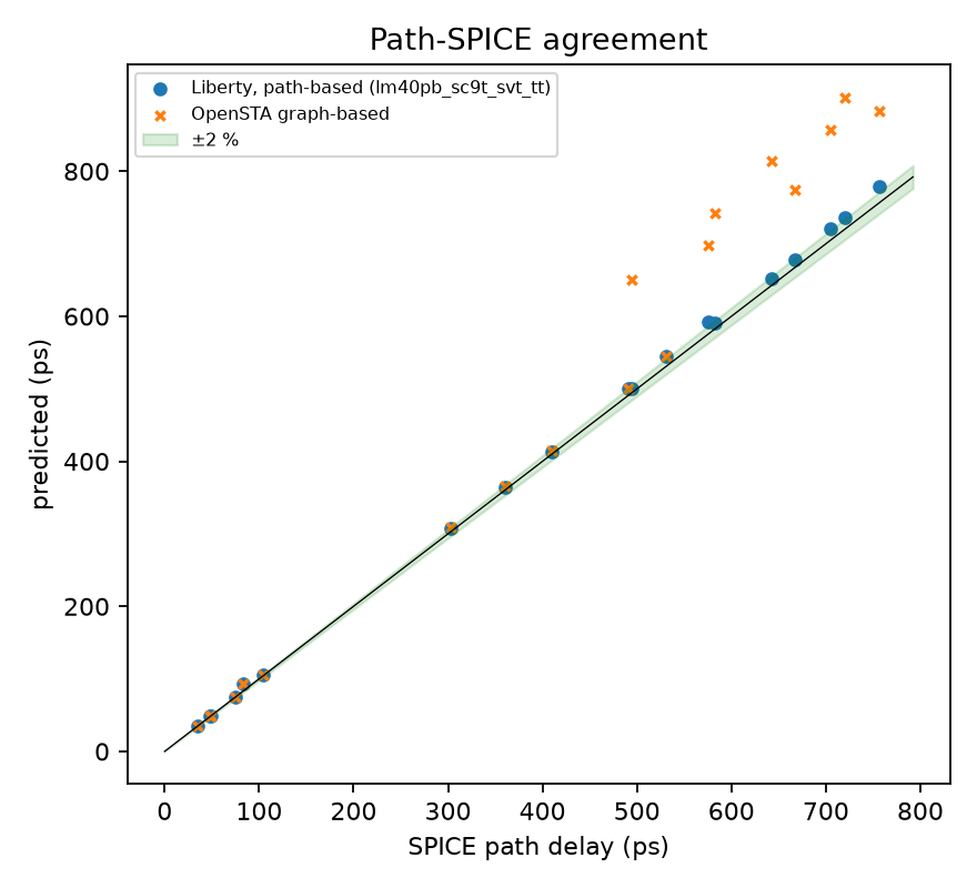
These checks also found and fixed real problems before release, among them XOR and MUX timing tables measured for one switching direction only, and AOI/OAI tables measured in their fastest input state. All are documented.
Featured analysis: aging
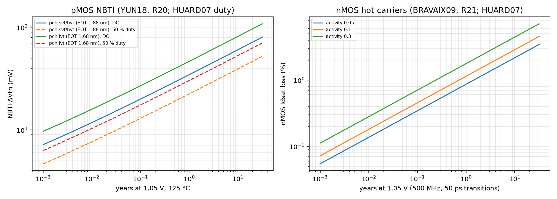
How much slower is a chip after ten years at 125 °C? We model the two main transistor wear-out mechanisms from published 40 nm-class measurements:
- Bias-temperature instability in pMOS, which raises the threshold voltage whenever the transistor is on;
- Hot-carrier injection in nMOS, which damages the transistor while it switches.
The degraded transistors are characterized into aged timing libraries that any timing tool can use directly. Ten years at nominal voltage shifts the pMOS threshold by about 40 mV in typical use and up to 60 mV under constant stress.
Built from
International roadmap tables (ITRS 2009), published 45 nm process papers, the FreePDK45 research kit, and peer-reviewed reliability measurements.
Interactive 3D cells
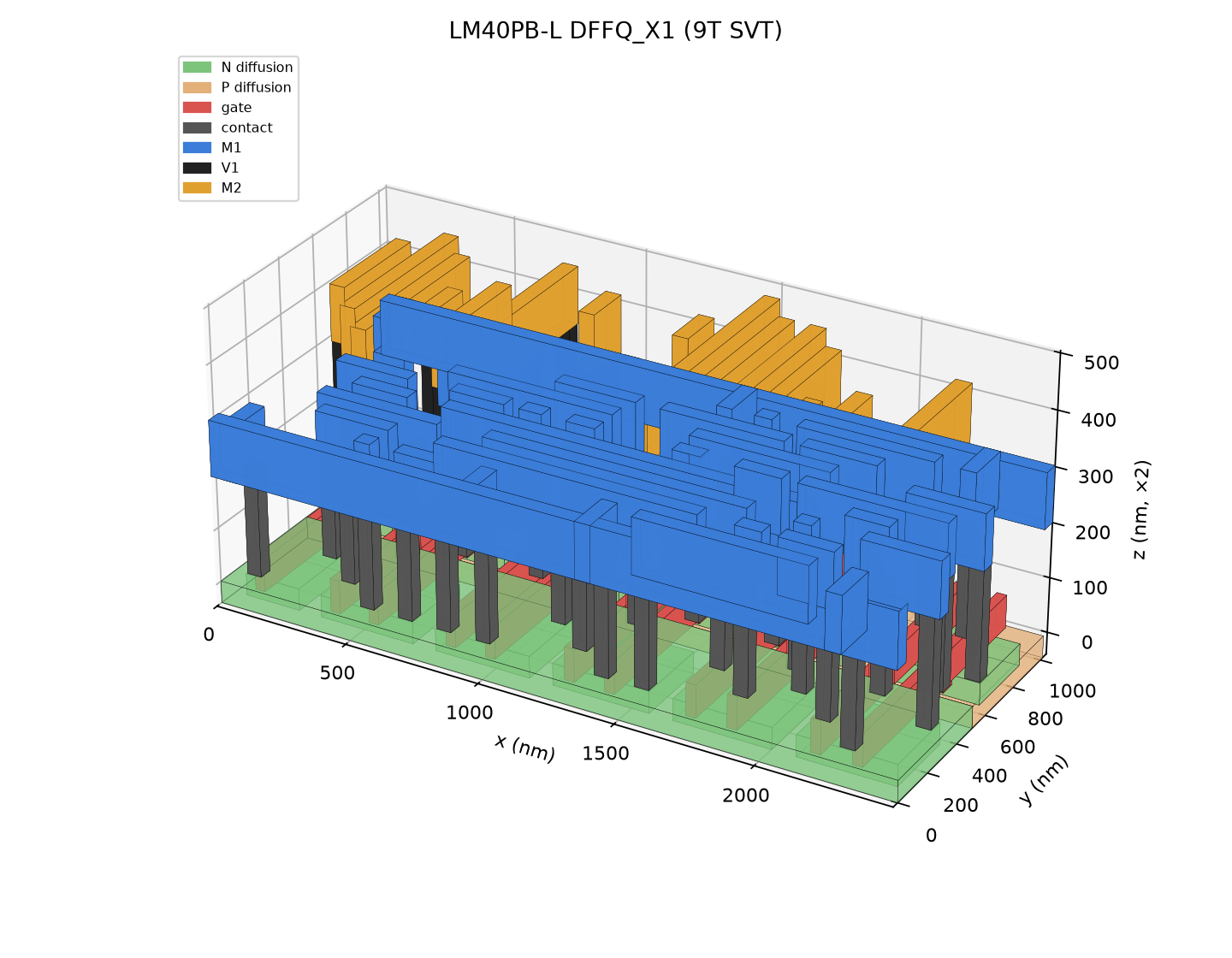
Generated cells, layer by layer at true heights. Pick a cell to load it.
Drag to rotate, scroll or pinch to zoom. Heights are drawn at 2× for legibility.