LM02NS-H
2 nm nanosheet, high performance / AI
Technology description in progress; device fit and cells next; backside power planned.
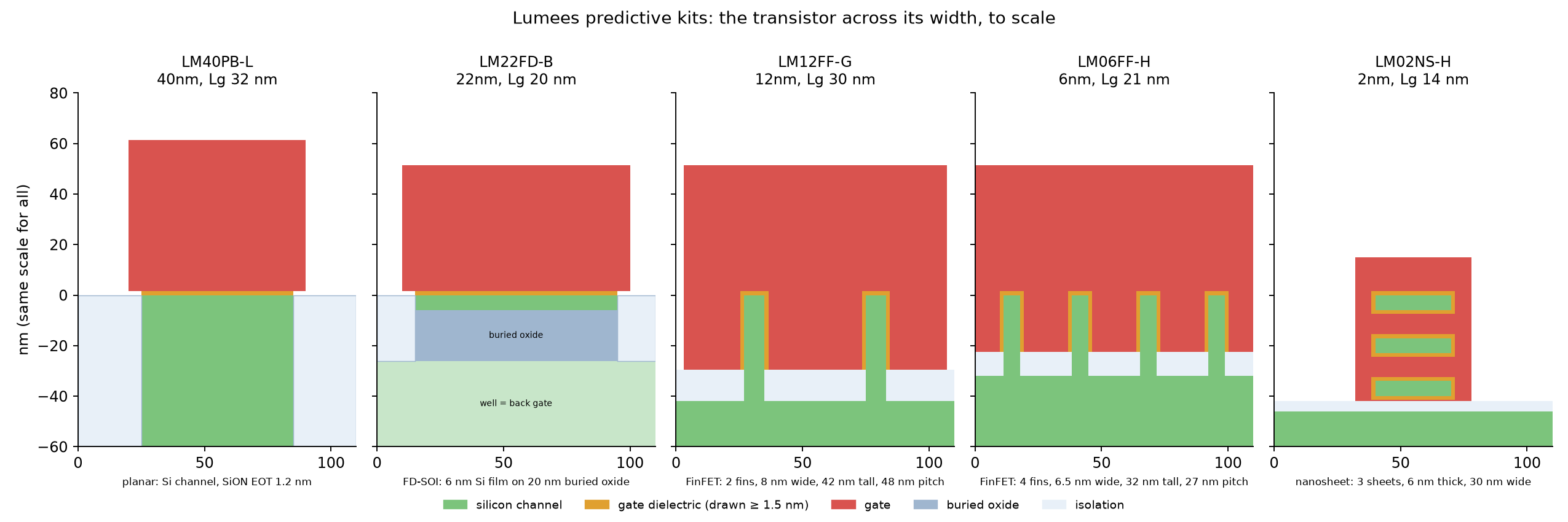
LM02NS-H is a 2 nm-class gate-all-around kit. Each transistor is a stack of three thin silicon nanosheets, 6 nm thick, fully surrounded by the gate. Wrapping the gate on all four sides gives the best electrostatic control of any transistor in the family, and sheet width is a design choice: wider sheets for performance, narrower for density. The description follows the IRDS 2024 roadmap for its "2 nm" generation and published nanosheet process papers.
Why 2 nm nanosheet
Gate-all-around nanosheets are the transistor of the leading edge, built for AI accelerators, data-centre processors and flagship mobile chips. They arrive together with other changes: power delivered from the back of the wafer, new interconnect metals and ever tighter cells. This is where design tools have to be ready first.
Technology at a glance
| Supply | 0.65 V nominal |
| Contacted gate pitch | 48 nm |
| Gate length | 14 nm |
| Nanosheets | 3 per device, 6 nm thick, 15 nm (dense) to 30 nm (performance) wide |
| Cell height | 120 nm (5 tracks) |
| Metal stack | M0 plus 16 routing layers; 22 nm M0 pitch, 24 nm lower-metal pitch |
| Threshold voltages | SVT, LVT, ULVT |
| Device model | BSIM-CMG (gate-all-around geometry) |
Interconnect
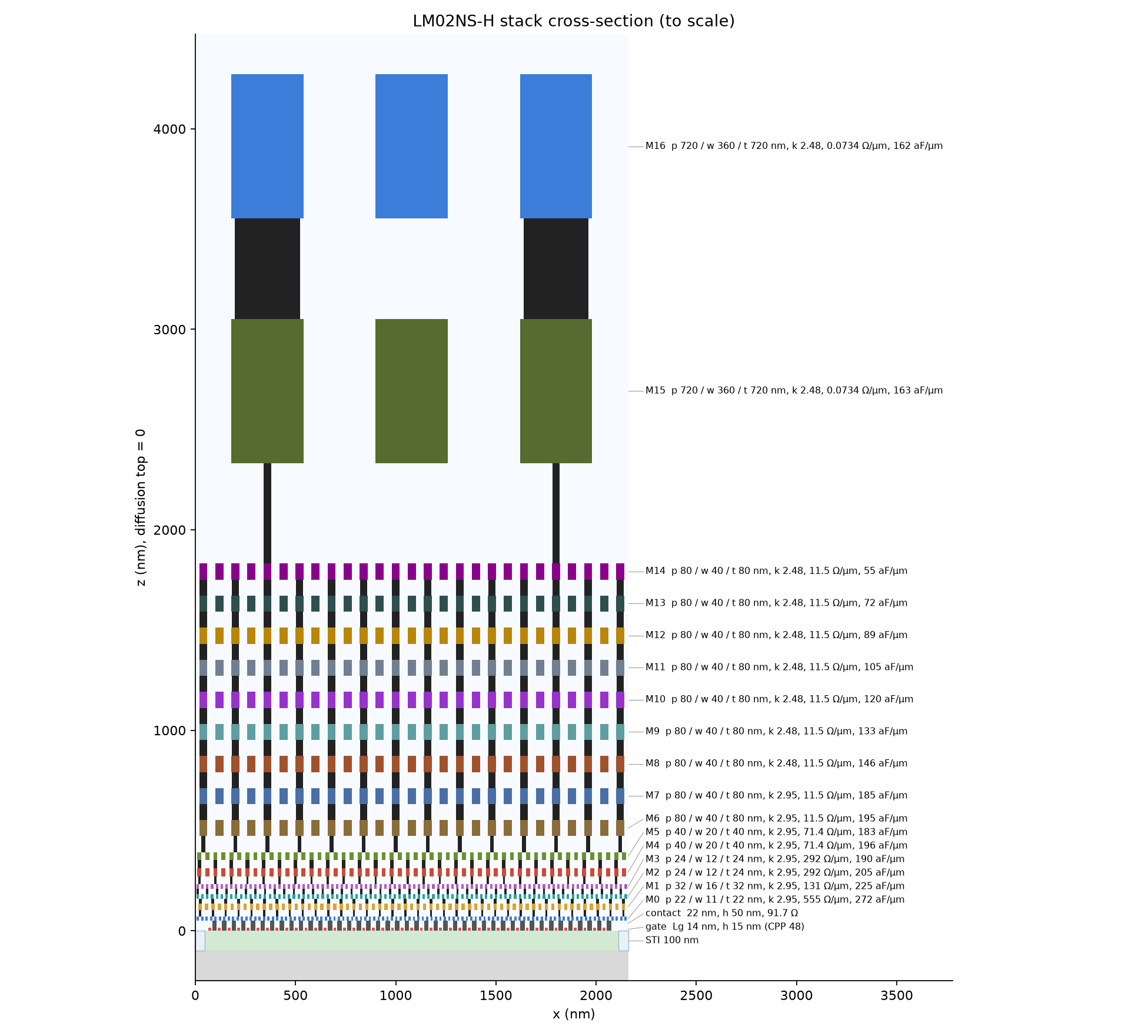
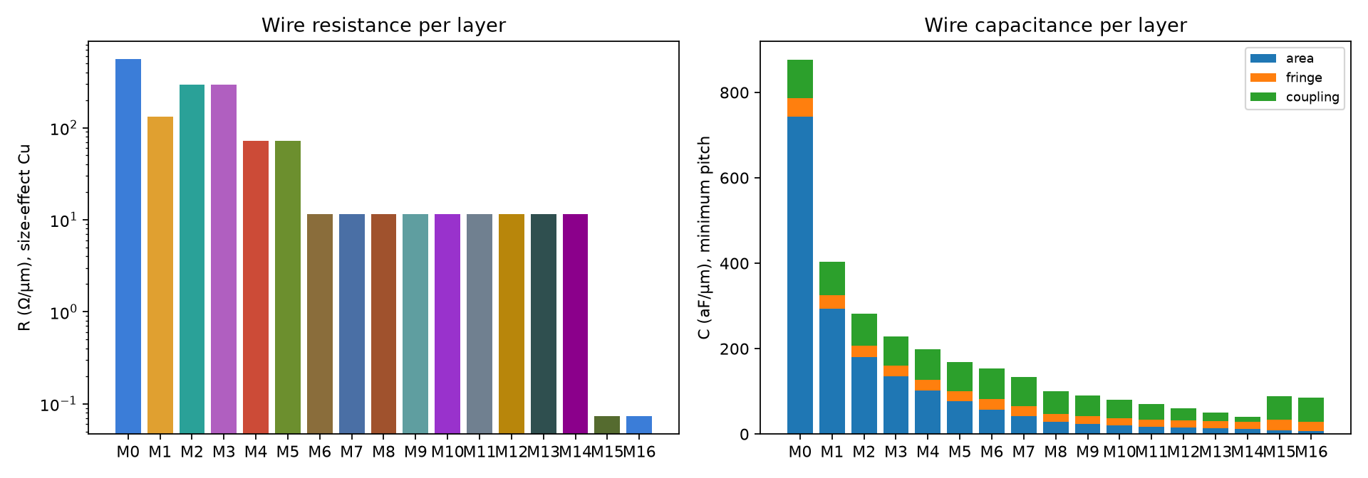
Sixteen routing layers above a 22 nm-pitch local layer (M0): M1 at 32 nm, two layers at 24 nm, two at 40 nm, nine at 80 nm and two thick power layers at 720 nm, following the IRDS 2024 roadmap. At 11–16 nm line width, wire resistance is 130–560 Ω per micrometre, which is why backside power delivery matters at this node.
Backside power delivery
At 2 nm, power is moving to the back of the wafer. In the IRDS 2024 roadmap's 2 nm generation, four backside metal layers (192 nm first pitch) deliver power and I/O through backside vias, freeing the front-side wiring for signals; the cell power rails remain on the front M0 and are fed from the back. We will build the kit in two variants, conventional front-side power and backside power, and compare voltage drop, density and wire resistance between them.
The family paper
LM02NS-H is the subject of our planned research paper: the method behind all five kits, and how the 2 nm kit's numbers line up with four other nodes built the same way. A 2 nm kit is far more credible when it sits at the end of a family checked against published data at every step.
Built from
The IRDS 2024 roadmap, published nanosheet and 2 nm process papers, a published 3 nm nanosheet cell-library study, studies of backside power delivery, and published resistivity data for nanometre-scale metals.
Next
Device fit on the perimeter-current basis the roadmap uses, standard cells at the 120 nm height, then the backside power variant.