LM06FF-H
6 nm FinFET, high performance
Technology description complete; device models fitted; libraries next.
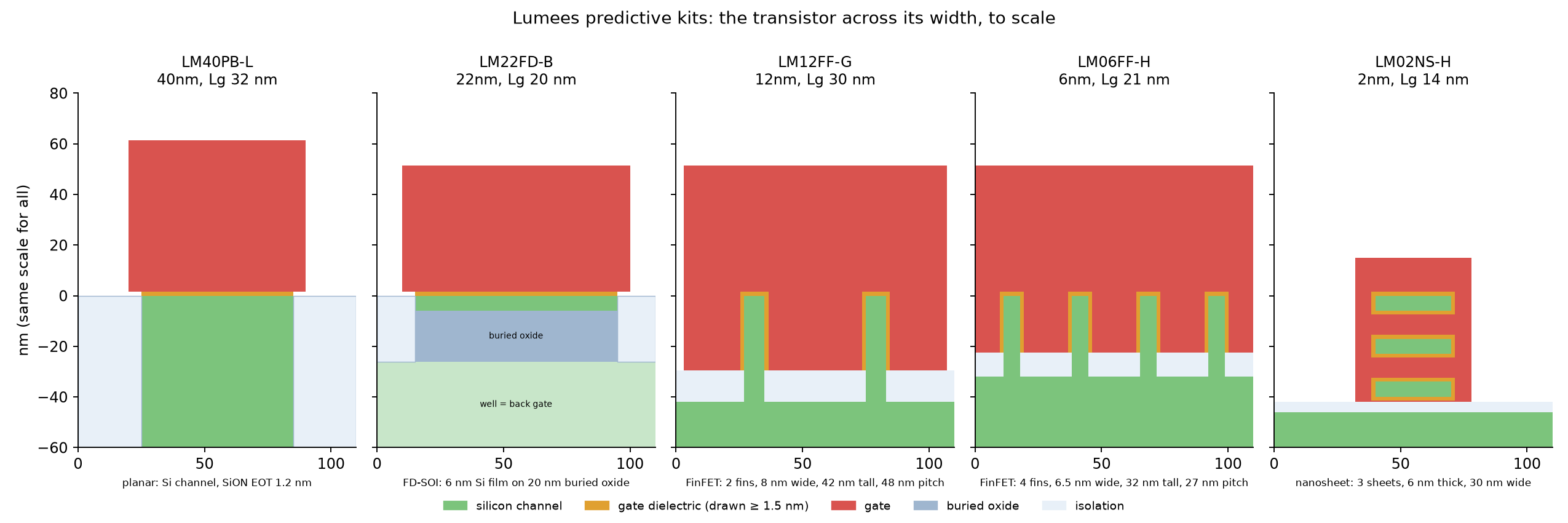
LM06FF-H is a 7/6 nm-class high-performance FinFET kit with an extreme-ultraviolet (EUV) patterned interconnect. Its front-end dimensions (54 nm gate pitch, 27 nm fin pitch) follow the well-known ASAP7 predictive research kit; its transistor targets, models, interconnect and libraries are our own, each cited.
Why 6 nm
The 7/6 nm class is where high-performance computing, mobile processors and AI accelerators moved in volume, and where interconnect resistance and transistor variability became first-order design problems. It is the last FinFET generation in our family before the move to gate-all-around.
Technology at a glance
| Supply | 0.7 V nominal |
| Contacted gate pitch | 54 nm |
| Gate length | 21 nm |
| Fin pitch / height / width | 27 / 32 / 6.5 nm |
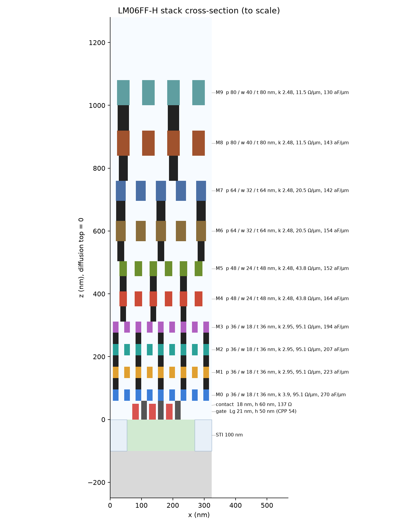
| Metal stack | 10 layers, 36 nm minimum pitch |
| Cell heights | 6 and 7.5 tracks |
| Threshold voltages | SLVT, LVT, RVT, plus SRAM devices |
| Device model | BSIM-CMG |
Transistors
| Device | Leakage (nA/µm) | Drive (µA/µm) |
|---|---|---|
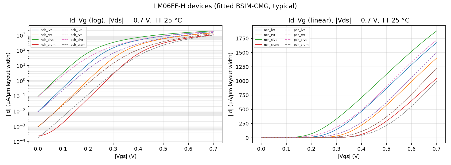
| nMOS SLVT / LVT / RVT | 90 / 9 / 0.7 | 1881 / 1674 / 1402 |
| pMOS SLVT / LVT / RVT | 89 / 8.5 / 0.85 | 1718 / 1500 / 1226 |
Currents are per micrometre of layout width.
Interconnect
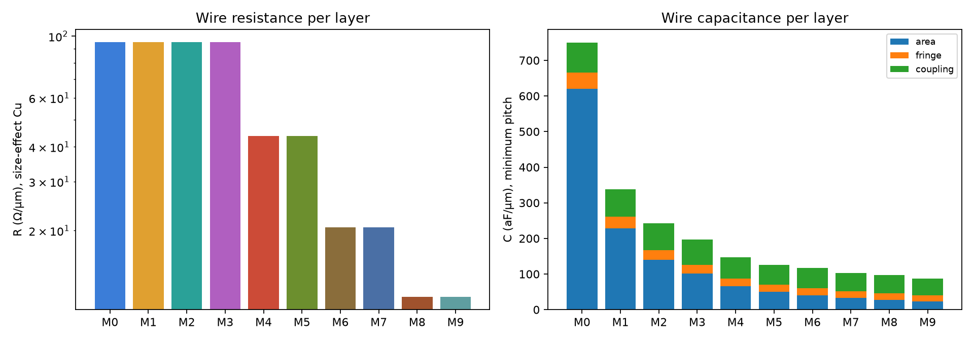
At 36 nm pitch, copper lines are only 18 nm wide, and their resistance is about 95 Ω per micrometre, roughly 17 times that of the 40 nm kit's narrowest wires. Our stack models that size effect layer by layer, and self-forming barriers that lower via resistance.
Featured analysis: variability and wire-dominated paths
At 6 nm, random variation between neighbouring transistors and the rising resistance of very narrow wires dominate timing. We will build statistical timing libraries and size-effect-aware wire models, and show which paths are limited by wires rather than by gates.
Built from
The ASAP7 research kit (front-end rules and device targets), the IRDS roadmap, and published studies of copper resistivity at nanometre widths.
Next
Standard-cell libraries at two heights and three threshold flavours, then characterization.