Five kits. 40 nm planar to 2 nm nanosheet.
Five process design kits, from 40 nm planar to 2 nm nanosheet, built from public data, with every number traceable to its source.
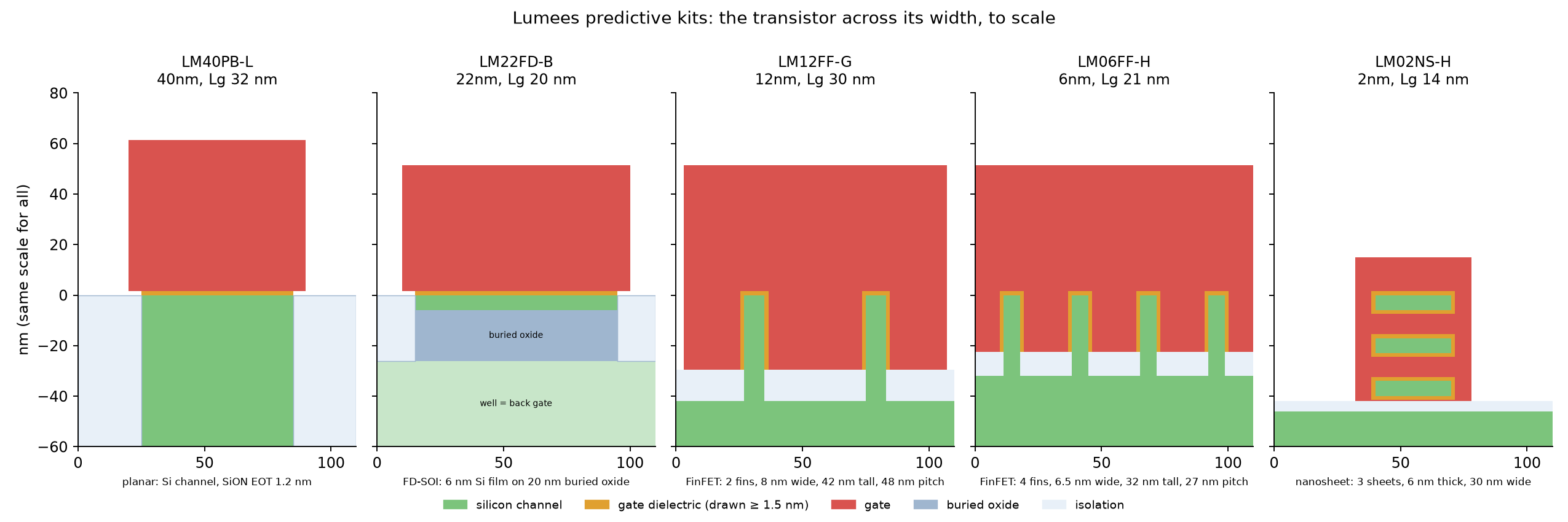
The family
A process design kit (PDK) is everything a chip designer needs to build on a technology: transistor models, standard-cell libraries, timing and power data, wiring rules and resistance and capacitance of every metal layer. Foundry PDKs are confidential, tied to one process and usually unavailable for research and tool development.
Lumees Lab builds its own predictive PDKs: complete, realistic kits for five technology generations, derived from published roadmaps and process papers. They are the technology foundation for our tools, including Lumina Spice (circuit simulation). We use them to develop, test and calibrate those tools on full designs without depending on any foundry.
The five kits span the four transistor architectures of the last fifteen years: planar bulk, fully depleted silicon-on-insulator, FinFET and gate-all-around nanosheets. Together they let us study how design behaviour changes from one generation to the next, using one method throughout.
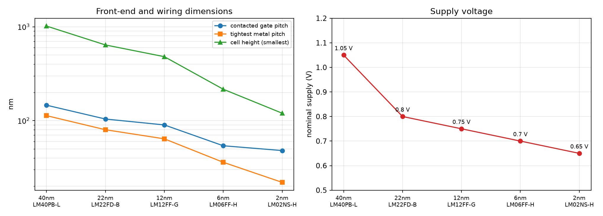
How we build them
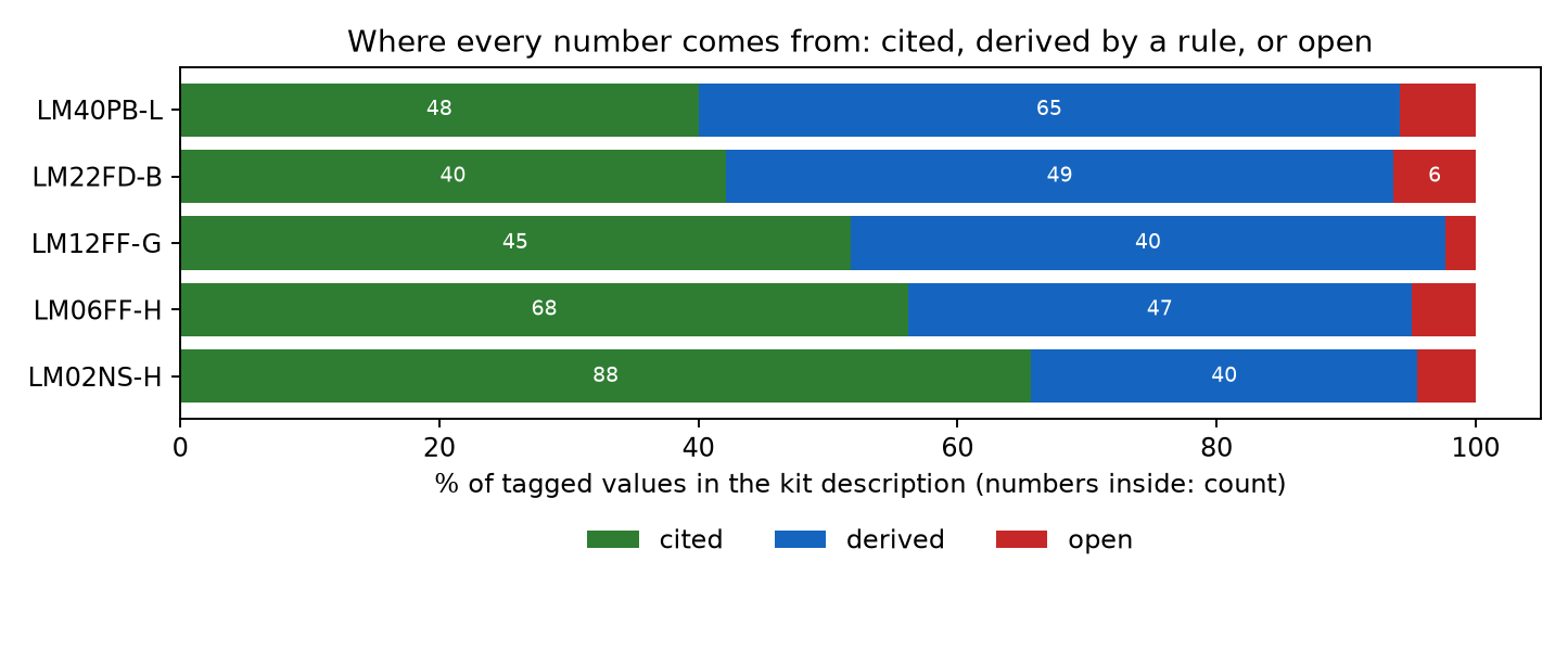
One cited description per kit. Each kit starts from a single technology description. Every value in it (supply voltage, gate pitch, oxide thickness, metal pitches, transistor targets) carries its origin:
- cited: taken from a roadmap (ITRS, IRDS), a published process paper, or a public research kit;
- derived: computed from cited values by a numbered, documented rule;
- open: not yet sourced, shown as such and tracked until it is.
Nothing is a silent default.
Generated, not hand-drawn. Transistor models are fitted to the cited targets. Standard cells are placed and routed by our own generator, which follows each kit's layout rules. Timing and power libraries are characterized from the netlists of the generated layouts, including their wiring parasitics.
Checked against independent references. Each kit is compared with published data it was not fitted to. Every library is checked cell by cell: logic function extracted from the drawn layout, layout rules, and timing against transistor-level simulation of real logic paths. Every error these checks have found is documented with its cause and fix.
Honest by design. These are predictive kits: realistic and internally consistent, but not calibrated to any foundry's silicon, and not a model of any specific commercial process.
What each kit contains
- Device models: BSIM4 (planar), BSIM-IMG (FD-SOI, with the back gate) and BSIM-CMG (FinFET, nanosheet), with process corners
- Standard-cell libraries: logic, sequential and physical cells, several threshold-voltage flavours and cell heights, drive strengths X1–X8
- Timing and power libraries (Liberty) across process, voltage and temperature corners
- Interconnect stack: every metal layer with size-effect resistivity and capacitance tables
- Design views: GDS layouts, LEF abstracts, technology LEF, CDL and SPICE netlists, Verilog models, layer maps
- A technical sheet per kit, generated from the kit's own data
Why wires matter more every generation
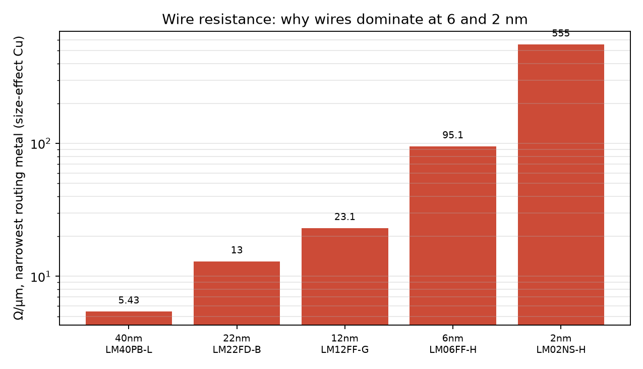
As wires shrink, their resistance per micrometre rises steeply: the metal cross-section falls and electrons scatter at the surfaces and grain boundaries. At 6 and 2 nm, many paths are limited by wires rather than transistors. Our kits model this size effect for every layer, so timing on the kits sees it too.
Research built on the kits
Each kit carries one featured analysis:
| Kit | Featured analysis |
|---|---|
| LM40PB-L | Aging: transistor wear-out and aged timing libraries |
| LM22FD-B | Back-bias compensation of aging and variation |
| LM12FF-G | Self-heating and temperature inversion |
| LM06FF-H | Variability (statistical timing) and wire-dominated paths |
| LM02NS-H | The 2 nm kit, its method, and backside power delivery |